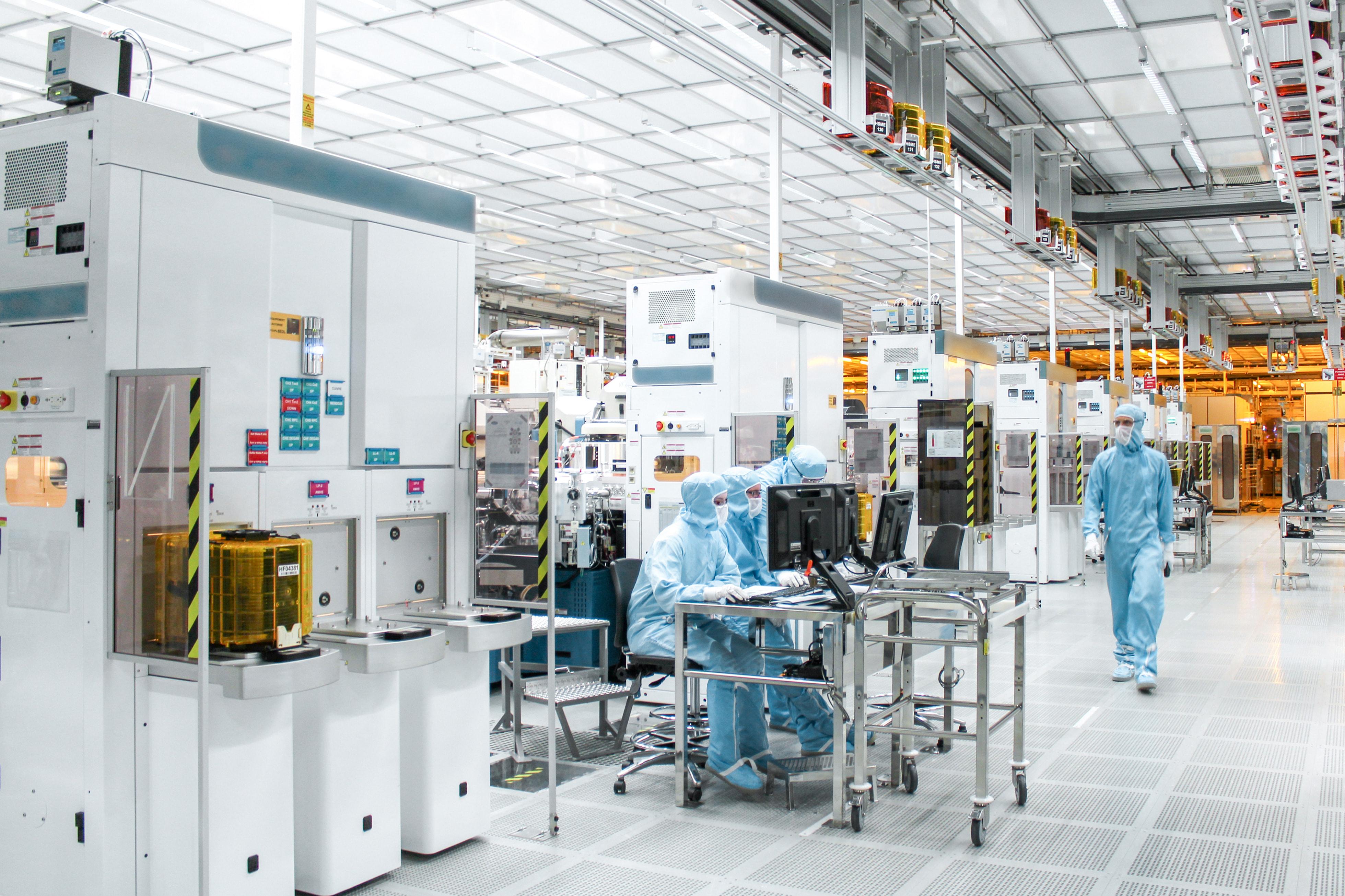
Application Description
Daisuki Advanced Technology provides detector solutions for wafer inspection and metrology systems used in semiconductor manufacturing. Our detectors support defect detection, dimensional measurement, alignment verification, optical inspection, and process monitoring with high sensitivity and stable performance. Designed for high-speed and high-resolution measurement requirements, our detector portfolio supports advanced inspection tools, research systems, and commercial semiconductor production equipment.
Recommended Detector Types
Click any detector type to browse available products.
Related Application Areas
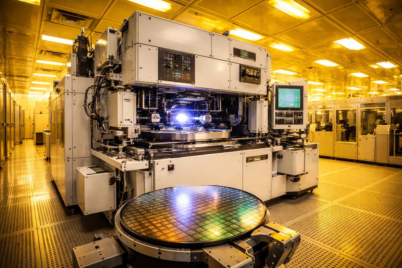
Lithography, UV/EUV & Plasma Monitoring
Daisuki Advanced Technology supplies detector solutions for lithography, ultraviolet, extreme ultraviolet, and plasma monitoring applications in semiconductor fabrication and advanced research. Our detectors support accurate measurement of UV/EUV intensity, plasma emissions, optical power, and process conditions. These solutions help customers improve process control, reduce production variability, and support precise monitoring in both research facilities and commercial semiconductor manufacturing lines.
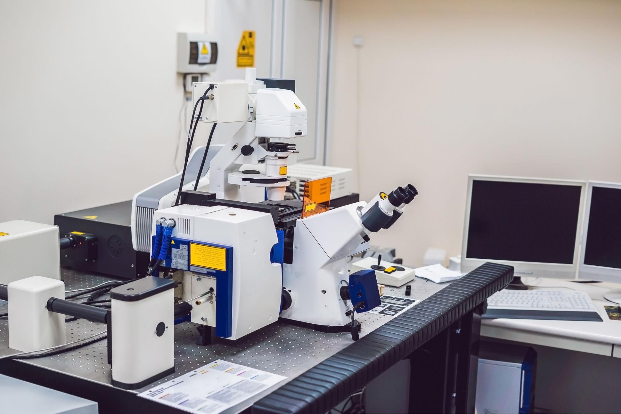
Imaging & Inspection Systems
Daisuki Advanced Technology provides detector solutions for imaging and inspection systems used in semiconductor inspection, industrial automation, electronics manufacturing, laboratory research, and quality control. Our detector portfolio supports high-resolution imaging, fast response, high sensitivity, wide dynamic range, and low-noise signal acquisition. We supply standard and customized detector options for customers requiring accurate image capture, reliable inspection performance, and stable long-term operation.
Need help selecting a detector?
Share your instrument requirements and Daisuki will help identify suitable detector options.
Request Consultation